PCB routing
WOGLAB – PCB routing
At WogLab, we implement exclusively manual PCB routing. This allows us to achieve maximum compliance with technical requirements and ensure reliable operation of devices even in the harshest conditions. Our process is based on deep engineering development of every aspect of the design. We take into account not only the requirements of the technical task, but also real operating conditions: temperature conditions, mechanical loads, electromagnetic environment.
When working on projects, we face various challenges of modern electronics. For high-frequency devices, special attention is paid to impedance control and minimization of crosstalk. In power circuits, heat flow distribution and conductor cross-section are carefully worked out. For multilayer high-density assembly (HDI) boards, special layout strategies are developed using microvias and blind holes.
“A printed circuit board is not just conductors on a substrate. It is a complex system, where each element affects the operation of the device. We design not to “pass the test”, but to operate flawlessly.”
It is important for us that the developed boards not only meet formal requirements. But also ensure stable operation of the equipment throughout its service life. That is why we pay special attention to such aspects as design maintainability, redundancy of critical circuits and ease of subsequent adjustment.
In the following sections, we’ll detail each step of our workflow. From pre-routing to special design cases, so you can fully appreciate our level of expertise in PCB design.
Detailed preparation for tracing
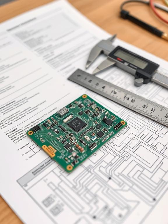
Before starting the design, our engineers analyze the circuit and technical requirements. Close attention is paid to every detail – from components to operating conditions.
Before starting the design, our engineers conduct a comprehensive analysis of the provided circuit diagram. This stage includes several important aspects. First, we carefully study the technical specifications, paying special attention to the operating conditions of the future device – temperature range, vibration loads, requirements for electromagnetic compatibility. Secondly, the circuit is analyzed to identify critical circuits: high-speed digital data transmission lines, sensitive analog paths, power circuits with high currents. Individual routing requirements are formed for each type of connection.
Particular attention is paid to the component base. We analyze each element for its characteristics: overall dimensions, heat dissipation, installation requirements. This allows us to foresee potentially problematic areas of the future board in advance.
Creation and verification of library components
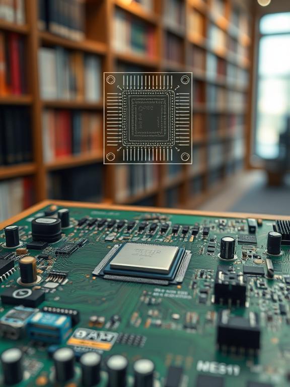
Our engineers carefully check each element before adding it to the library.
Developing a component library is a fundamental stage, which largely determines the quality of the final result. Our specialists create footprints taking into account many key factors. The geometry of the contact pads is carefully worked out, taking into account the features of soldering – both manual and automated. For components with high heat generation, special thermal pads are developed to ensure effective heat dissipation.
Each footprint undergoes a multi-stage check. We analyze compliance with the actual dimensions of the component, the correct placement of markings, and the convenience of subsequent installation. For all components, 3D models are created, allowing potential collisions with the case or other structural elements to be identified at the design stage.

Creation and verification of library components
Our engineers carefully check each element before adding it to the library.

Optimization of printed circuit board structure
Our engineers select the optimal base materials and layer configuration. This ensures the ideal combination of performance and cost of your product.
Determining the optimal PCB stack-up structure is a complex engineering task that requires a comprehensive approach. Our specialists take into account many interrelated factors. The number of signal layers is determined based on the complexity of the circuit and the installation density. For high-speed devices, we provide dedicated power and ground layers. This ensures high-quality shielding, return current paths, and parameter stability.
Particular attention is paid to the distribution of circuits across layers. We group signals by their types and sensitivity, minimizing mutual interference. For multilayer boards, the alternation of signal and plane layers is carefully worked out. This is especially important to ensure the integrity of the power supply of high-speed digital components.
Manual PCB routing
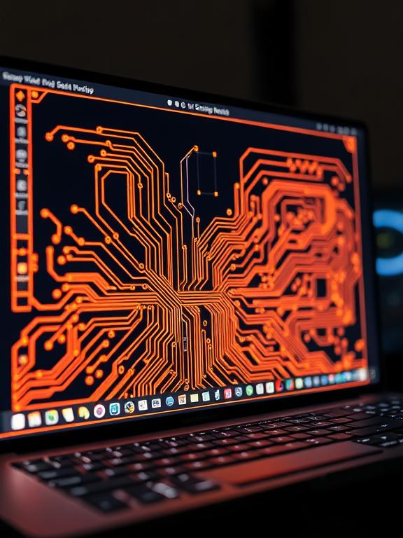
PCB routing is a lengthy process, where each conductor on the board is laid manually, taking into account many technical nuances. For analog circuits, we ensure the minimum length of connections and their protection from digital interference. Signal paths are designed taking into account the wave resistance, which is especially critical for high-speed interfaces.
When routing power supply circuits, we pay special attention to current distribution, minimizing voltage drops and ensuring the stability of the power supply for all components. For this, special methods are used to calculate the cross-section of conductors and the optimal placement of decoupling capacitors.

Manual PCB routing

Comprehensive quality control
After the routing is completed, a comprehensive design check is performed. We perform a visual inspection of the layout, analyzing the uniformity of the conductor distribution and the absence of overstressed areas. Particular attention is paid to the compliance of the routing with the original schematic diagram – each circuit, each contact is checked.
Technological control includes checking compliance with all production standards and DFM/DFA compliance: minimum distances between elements, via sizes, solder mask requirements. For critical nodes, thermal modeling is additionally performed, allowing to identify potential overheating.

Special design cases
Our engineers develop solutions for the most complex tasks: high-frequency boards, products for extreme temperatures and other special operating conditions.
When working with special-purpose boards, we use additional methods. HDI boards use micro-hole and blind-via technology, which requires a special approach to routing. Hybrid boards take into account different thermal expansion coefficients of materials. High-voltage boards are designed with all necessary air and surface gaps.
The result of our work is a fully production-ready printed circuit board, where each track is laid with a full understanding of its impact on the operation of the entire device. We guarantee that the routing we have developed will ensure stable and reliable operation of your product under the stated operating conditions.

Special design cases
Our engineers develop solutions for the most complex tasks: high-frequency boards, products for extreme temperatures and other special operating conditions.
At Woglab we guarantee
Professional PCB routing

PCB routing is a multi-stage process that requires deep knowledge, precision and an individual approach to each project.
Our routing is not just laying out tracks. It is a complex of engineering solutions that guarantee reliability, minimal interference and compliance with technical requirements. Woglab takes on even the most complex tasks, providing a turnkey result – from the scheme to the finished product.
Want a perfectly laid out board? Leave a request – let’s discuss your project!
