WOGLAB – PCB design, development of printed circuit boards of any complexity
Quality assurance, compliance with standards, support at all stages.
Request an estimate
Contact us for PCB design


About us
Professional PCB design
Woglab provides professional services in the field of design and routing of printed circuit boards (PCB). Our team has extensive experience in creating complex devices for various purposes.
Our main activity is the development of high-tech printed circuit boards for critical applications. We have unique experience in designing high-frequency boards for telecommunications equipment, multilayer boards with high mounting density (HDI), specialized solutions for the aerospace and medical industries.
Woglab is not just an executor, but a technology partner that takes on the most complex tasks in the field of printed circuit board design.
We are ready to become a reliable link in your production chain, ensuring consistently high quality and meeting deadlines.
Our services
Professional PCB Design

PCB Routing
WogLab offers a full cycle of PCB design with an emphasis on high-density layout, electromagnetic compatibility and optimal performance. Our solutions are suitable for devices of any complexity level – from consumer electronics to aerospace systems.

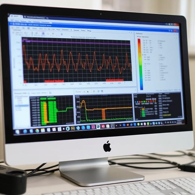
Signal and Power Integrity (SI/PI) Analysis
WogLab offers comprehensive simulation to ensure your devices operate reliably, performing detailed signal integrity (SI) and power integrity (PI) analysis at the PCB design stage to eliminate errors that reduce the reliability and performance of electronics.

Design documentation preparation
WogLab provides a full cycle of project documentation support according to GOST, IPC and international standards – from the development of schemes to the formation of a file package for serial production. Our services guarantee compliance with standards and minimize risks at the stage of manufacturing and assembly of printed circuit boards.
Additional services
Consulting and engineering support at all stages
WogLab offers end-to-end project support, from concept to serial production. “Engineering as a Service” allows you to scale your team without hiring additional specialists, gaining access to experts in the field of PCB design, validation, and production.

Why choose WOGLAB
Advantages that make us a reliable partner in the development and production of printed circuit boards
Expertise and experience
WogLab brings together a team of certified engineers with 10+ years of experience in designing printed circuit boards of any complexity.
Full cycle of services
Comprehensive solutions for your project: design, routing, analysis, documentation and production support.
Quality guarantees
Strict control at every stage: compliance with standards, design verification and prototype testing for a flawless result.
Flexible working formats
We will adapt to your needs: from one-time consultations to a dedicated engineer for a project with reporting and transparent pricing.
Technological equipment
We design in professional CAD systems (Altium, Mentor), ensuring the accuracy of calculations and compliance with real operating conditions.
Customer focus
Your success is our priority: we work under NDA, comply with all requirements and offer project audit for accurate calculation of deadlines and budget.